PCB antenna processing
Introduction
PCB antennas have become an essential component in the ever-evolving wireless communication technologies. Widely used in various industries, from aerospace and defense to consumer electronics, PCB antennas serve as a key element in transmitting and receiving signals, allowing for efficient and reliable communication.
In this article, we will delve into the world of PCB antennas, looking at their structure, operation, and processing techniques.
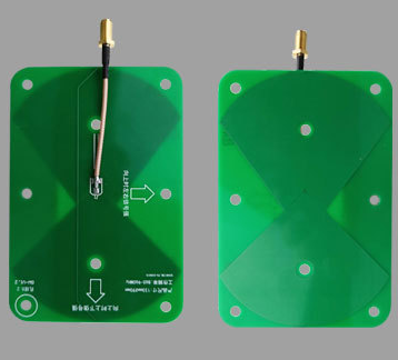
PCB Antenna: Structure and Design
A PCB antenna is essentially a conductive trace on a printed circuit board. The trace is designed to radiate electromagnetic waves and receive signals at specific frequencies. The physical structure of the antenna can significantly impact its performance. The size, shape, and alignment of the antenna all play a crucial role in the antenna's effectiveness.
The commonly used PCB antennas are monopole antennas, loop antennas, and patch antennas. A monopole antenna consists of a ground plane with a single vertical conductor, while a loop antenna consists of a single loop of conductor. A patch antenna consists of a radiating patch and a ground plane.
PCB Antenna: Operation and Characteristics
The PCB antenna's fundamental operation is based on the principle of electromagnetic radiation. The AC current flowing through the conductive trace generates an electromagnetic field, which radiates energy in the form of waves. The antenna's size, shape, and material determine its resonant frequency, bandwidth, and radiation pattern.
The radiation pattern refers to the shape of the electromagnetic field that is emitted by the antenna. The pattern can be directional, where energy is concentrated in a specific direction, or omni-directional, where energy is evenly distributed in all directions. The antenna's radiation pattern is key in determining its gain, which is a measure of how effectively the antenna can transmit or receive energy.
PCB Antenna: Processing Techniques
The processing techniques used in PCB antenna fabrication significantly impact the antenna's performance. The techniques used vary depending on the antenna's design, the materials used, and the intended application.
The most common processing techniques used in PCB antenna fabrication are chemical etching, laser ablation, and milling. Chemical etching involves removing unwanted copper from the board using a PCB etchant solution. Laser ablation uses a laser to vaporize or burn away the unwanted copper. Milling involves removing unwanted copper using a cutting tool.
The choice of processing technique depends on several factors, such as the cost, the complexity of the antenna design, and the tolerances required.
Conclusion
In conclusion, PCB antennas have become an essential component in the modern world of wireless communication technologies. Their structure, operation, and processing techniques are all critical factors in determining their effectiveness. As wireless communication technologies continue to evolve, so will the need for innovative and efficient PCB antenna designs and processing techniques.
