Design of PCB WiFi Antenna
1、 Preface
In the context of the popularization of the Internet today, the application of wireless networks is becoming increasingly widespread. In wireless networks, WiFi is the most common type. When making WiFi devices such as routers, wireless cameras, WiFi modules, etc., the design of the antenna is crucial. This article will delve into the design principles and optimization methods of PCB wifi antennas.
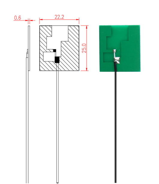
2、 Design principle of PCB wifi antenna
The design of PCB wifi antennas is a complex discipline. During the design process, issues such as power, impedance, frequency, etc. need to be considered. Taking the 802.11b/g/n standard device as an example, its frequency range is 2.4-2.5GHz, and the impedance of the antenna must be 50 ohms. At the same time, the antenna also needs to ensure high efficiency and low distortion.
After determining the polarity of the antenna, considerations include the length, shape, and height from the ground of the antenna. Generally speaking, the antenna length is less than or equal to λ/ 4. The shape can be a straight line or a polyline, and the higher the height from the ground, the higher the radiation efficiency.
3、 Optimization Method for PCB WiFi Antennas
3.1 Integration into PCB production process
PCB wifi antennas can be directly realized through the PCB production process, which can reduce manufacturing costs and improve manufacturing efficiency. At the same time, the antenna and circuit board can also be combined to improve overall efficiency.
3.2 Optimizing Antenna Shape
The shape of the antenna is a key factor affecting radiation efficiency. Optimizing the shape of the antenna can improve its efficiency and enhance signal transmission capability. For example, using broadband antennas and combining microstrip lines can achieve better antenna performance.
3.3 Considering circuit board layout
The layout of the circuit board also affects the performance of the antenna. To avoid collision between the antenna and the signal, we need to keep the antenna away from other components and try to separate the power and signal lines as much as possible. In addition, it is also necessary to improve the efficiency of the antenna through the ground area.
4、 Conclusion
This article explores the design principles and optimization methods of PCB wifi antennas, and summarizes that incorporating PCB production processes, optimizing antenna shape, and considering circuit board layout can significantly improve antenna efficiency. Therefore, when making WiFi devices, we need to carefully consider the design and optimization of the antenna to improve the stability and transmission rate of the wireless network.
