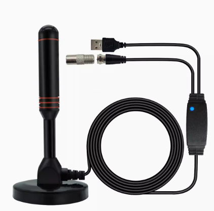
Bluetooth PCB antenna application
Bluetooth technology has become ubiquitous in recent years, with applications ranging from wireless headphones to smart home devices. One vital component of Bluetooth systems is the PCB (printed circuit board) antenna. This article will explore the operating principles of Bluetooth PCB antennas, their design considerations, and how to optimize their performance.
Bluetooth operates in the 2.4 GHz ISM (Industrial, Scientific, Medical) frequency band, and its antennas must be designed accordingly. The most common type of Bluetooth antenna is the PCB antenna on the board itself. It is a small, directional antenna that uses a printed circuit board as the radiating element. Because the antenna is integrated into the PCB, it has many advantages over other types, such as compact size, low cost, easy assembly, and high flexibility.
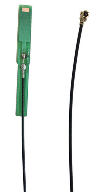
There are two basic types of PCB antennas: monopole and dipole. A monopole antenna is a single wire, while a dipole antenna consists of two wires arranged side by side. The choice between the two depends on the specific application and the board's size available. In general, smaller boards use monopole antennas while larger ones use dipole.
One key aspect of designing a PCB antenna is the layout. The length, width, and spacing of the PCB traces determine the impedance of the antenna. The impedance must match the impedance of the Bluetooth chip output, typically 50 or 75 ohms, to achieve maximum power transfer. Additionally, the location of the antenna needs to avoid blocked areas, ground planes, and other components that could interfere with its operation.
The shape of the PCB antenna also plays an important role in its performance. A popular design is the inverted F antenna because it uses a minimal amount of space but still provides good radiation efficiency. Its shape is similar to an L-shape, with a stub added to the top of the vertical line. Another shape is the meandered line antenna, which involves folding the trace back and forth to create a longer radiating element within the available board space.
Once the PCB antenna is designed, its performance needs to be tested and optimized. The key parameters include return loss, VSWR (voltage standing wave ratio), gain, and radiation pattern. Return loss measures how much RF power reflected back to the transmitter rather than radiated by the antenna. VSWR reflects how well the transmitter and antenna are matched together. Gain measures how much power the antenna radiates in a specific direction. Radiation pattern indicates the coverage area of the antenna.
To optimize the performance of the PCB antenna, several methods can be used, such as antenna tuning, impedance matching, and radiation pattern shaping. Antenna tuning involves adjusting the physical shape of the antenna to achieve the desired resonant frequency. Impedance matching can be achieved by adding a matching network, such as a series and parallel resistance-capacitance (RC) configuration or an inductor-capacitor (LC) circuit. Radiation pattern shaping can be achieved by adding reflective elements, such as a chip reflector or a printed reflector, to redirect the energy in a specific direction.
In conclusion, Bluetooth PCB antennas are essential components in Bluetooth systems that must meet specific design considerations to achieve optimal performance. The operating principles, design considerations, and performance optimization techniques have been discussed in this article to provide a comprehensive understanding of this technology. With the right design and optimization, PCB antennas can provide robust wireless connectivity for a wide range of Bluetooth applications.
