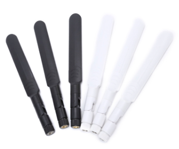
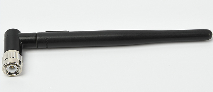
The manufacturing process and advantages of PCB antennas
Printed Circuit Board Antenna Fabrication and Its Advantages
Introduction
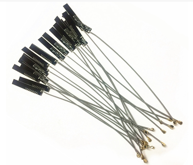
With the increasing demand for high-speed data transfer and connectivity in various electronic devices, the role of an antenna in wireless communication systems has become paramount. Antennas have undergone a significant transformation over the years from the traditional wire antennas to advanced Printed Circuit Board (PCB) antennas. PCB antennas have gained popularity due to their flexibility, ease of fabrication, low cost, compact size, and superior electrical performance.
PCB Antenna Fabrication
PCB antennas are designed by integrating a metal trace onto the PCB substrate, forming a conductive pattern. The metal trace is shaped based on the desired antenna type, including patch, monopole, dipole, and loop antennas. The PCB material and thickness are carefully selected based on the antenna's frequency range, gain, and bandwidth requirements. The fabrication process involves several steps, including:
1. Designing: The antenna's dimensions, metal trace shape, and substrate material are determined based on the desired electrical parameters.
2. PCB layout: Using PCB design software, the metal trace pattern is designed and adjusted to achieve the desired electrical characteristics.
3. Printing: The metal trace design is printed onto the substrate layer using high-precision printers.
4. Lamination: The substrate layer is laminated with the metal trace layer, providing a stable and durable antenna structure.
5. Cutting: The final antenna shape is cut from the PCB substrate, including any necessary electrical connections.
Advantages of PCB Antennas
1. Low cost – PCB antennas are designed by integrating the antenna onto the PCB substrate, reducing the component count and cost.
2. Compact size – PCB antennas are compact and easily integrated into electronic devices, providing space-saving advantages over traditional antennas.
3. Flexibility – With PCB technology, it's easy to modify and iterate antenna designs, increasing agility and flexibility.
4. Performance – PCB antennas offer excellent electrical performance, with high efficiency, gain, and bandwidth.
5. Multiple signal support – PCB antennas can be designed to support multiple signals, including GPS, Wi-Fi, Bluetooth, and LTE.
Challenges of PCB Antennas
Despite the many advantages of PCB antennas, there are some challenges associated with their designs:
1. Frequency limitations – PCB antennas typically operate in the range of a few hundred megahertz to several gigahertz, limiting their use in lower or higher frequency applications.
2. Signal interference – PCB antennas can suffer from signal interference from nearby components or electronic devices, negatively impacting performance.
3. Complex design – PCB antennas require careful design and optimization to achieve the desired electrical performance, often requiring advanced simulation and modeling software.
Conclusion
The popularity of PCB antennas continues to grow as the demand for wireless communication and connectivity increases. The combination of low cost, compact size, and excellent electrical performance makes PCB antennas ideal for various applications, including smartphones, tablets, laptops, and IoT devices. PCB antenna designs continue to evolve, providing new solutions for more complex and demanding applications.
